What is Semiconductor Plating DSA?
Semiconductor Plating DSA is a highly efficient and reliable plating system designed for the semiconductor industry.
It provides precise control and invariant plating of colorful accoutrements onto semiconductor substrates, icing high- performance and high- quality products.
It utilizes advanced technology and chemistry to deposit thin layers of essence or other accoutrements onto semiconductor substrates. It's grounded on the principle of electroplating, where an electric current is passed through a result containing the asked material, performing in a deposit of the material onto the substrate. The system consists of colorful factors, including a plating bath, power force, and controlunit.It provides precise control and invariant plating of colorful accoutrements onto semiconductor substrates, icing high- performance and high- quality products.
It offers cutting-edge digital switching technology for demanding semiconductor manufacturing applications that require ultra-precise process control and nanometer-scale tolerances.
The core DSA (Digital Switching Amplifier) enables real-time current tuning needed for super-uniform plating deposition. Advanced anode activation methods accelerate plating speeds. Robust hardware components stand up to rigorous 24/7 production environments.
Intuitive touchscreen interface allows easy monitoring and adjustment of plating parameters. The modular and reconfigurable system can scale up to meet increased production capacity needs.
With thousands of worldwide installations, our Semiconductor Plating solutions have a proven track record satisfying the stringent requirements of leading chipmakers. We have extensive experience tailoring our plating technology for wafer bumping, redistribution layer fabrication, TSV metallization, and other advanced IC packaging and interconnect processes.
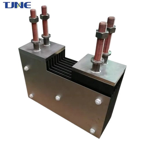
System Components
-
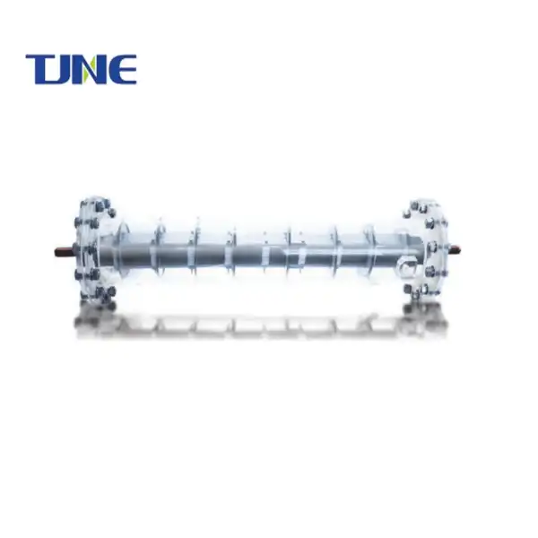
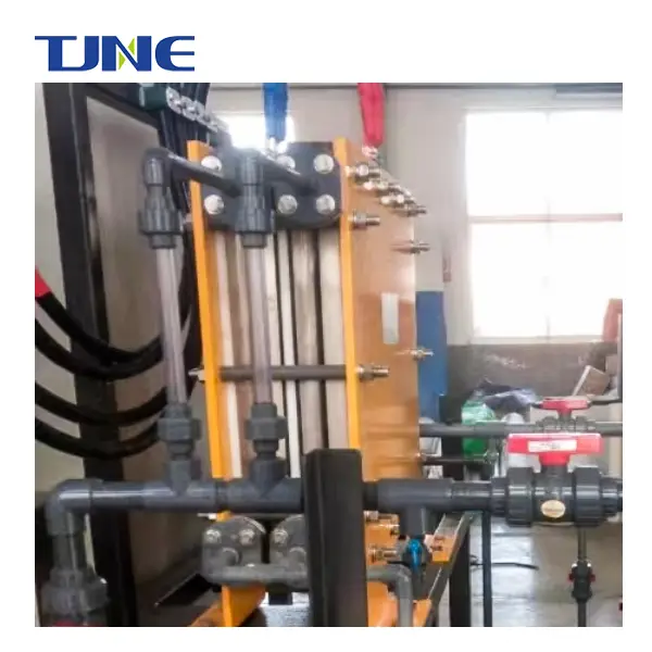
Plating bath: A container filled with the plating solution.
-
Power supply: Provides the necessary electric current for the plating process.
-
Control unit: Regulates the plating parameters, such as voltage and current, to ensure precise and uniform deposition.
-
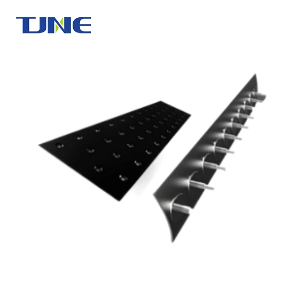
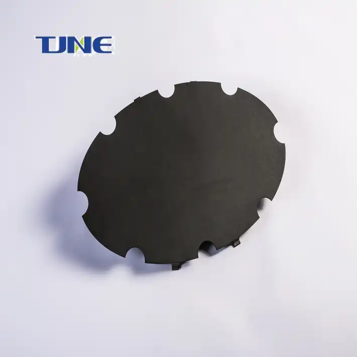
Electrodes: The anode and cathode used for the plating process.
-
Chemicals: Various chemicals are used in the plating bath to control the plating process.
Performance Parameters:
| Parameter | Value |
|---|---|
| Plating Rate | Up to 10 microns per minute |
| Plating Uniformity | Within 2% variation across the substrate |
| Plating Thickness Control | Accurate within 0.1 microns |
| Deposition Quality | High-density and void-free |
Technical Parameters
| Parameter | Value |
|---|---|
| Dimensions | 1500mm x 1000mm x 2000mm |
| Weight | 500kg |
| Power Consumption | 10kW |
| Voltage | 220V |
Economic Indicators
Semiconductor Plating DSA offers cost-effective solutions for the semiconductor industry. The plating system reduces material waste and ensures high yield, leading to significant cost savings.
Features and Advantages
-
Precise and uniform plating
-
High plating rate
-
Accurate thickness control
-
High-quality deposition
-
Cost-effective
-
Reliable and efficient
Applications:
It is widely used in the semiconductor industry for various applications, including:
(1)Integrated Circuits (ICs) Production
The Semiconductor Plating system enables high-precision copper electroplating for on-chip interconnects and redistribution layers in IC fabrication. Its stable current delivery and temperature controls deposit uniform copper layers with excellent conductivity meeting the demands of advanced ICs.
(2)Semiconductor Device Packaging
The system allows targeted plating of copper pillars, bumps and through-silicon vias (TSVs) during wafer-level, chip-scale and 3D packaging processes. Tight process controls prevent voids and enable reliable flip-chip assemblies.
(3)Wafer Fabrication
The Semiconductor Plating system is ideal for copper seed layer deposition, copper pillar bump plating, and TSV metallization during silicon wafer fabrication. It can also be used for plating solder bumps and tin-silver finish layers with excellent uniformity.
(4)Thin-Film Deposition
With its precise current delivery and solution agitation, the system deposits uniform thin-films of copper, gold, silver, tin and other metals for wafer-level redistribute layers, interconnects, and device structures with nanometer-scale tolerances.
FAQ:
1. Can I use Semiconductor Plating for plating non-semiconductor materials?
No, it is specifically designed for semiconductor plating applications and may not be suitable for other materials.
If you are considering Semiconductor Plating DSA for your requirements, please feel free to contact us at yangbo@tjanode.com. We are a professional manufacturer and supplier, offering strong technical expertise, comprehensive after-sales service, and fast delivery.