- English
- French
- German
- Portuguese
- Spanish
- Russian
- Japanese
- Korean
- Arabic
- Greek
- German
- Turkish
- Italian
- Danish
- Romanian
- Indonesian
- Czech
- Afrikaans
- Swedish
- Polish
- Basque
- Catalan
- Esperanto
- Hindi
- Lao
- Albanian
- Amharic
- Armenian
- Azerbaijani
- Belarusian
- Bengali
- Bosnian
- Bulgarian
- Cebuano
- Chichewa
- Corsican
- Croatian
- Dutch
- Estonian
- Filipino
- Finnish
- Frisian
- Galician
- Georgian
- Gujarati
- Haitian
- Hausa
- Hawaiian
- Hebrew
- Hmong
- Hungarian
- Icelandic
- Igbo
- Javanese
- Kannada
- Kazakh
- Khmer
- Kurdish
- Kyrgyz
- Latin
- Latvian
- Lithuanian
- Luxembou..
- Macedonian
- Malagasy
- Malay
- Malayalam
- Maltese
- Maori
- Marathi
- Mongolian
- Burmese
- Nepali
- Norwegian
- Pashto
- Persian
- Punjabi
- Serbian
- Sesotho
- Sinhala
- Slovak
- Slovenian
- Somali
- Samoan
- Scots Gaelic
- Shona
- Sindhi
- Sundanese
- Swahili
- Tajik
- Tamil
- Telugu
- Thai
- Ukrainian
- Urdu
- Uzbek
- Vietnamese
- Welsh
- Xhosa
- Yiddish
- Yoruba
- Zulu

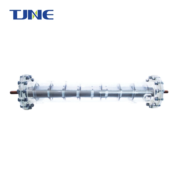
PCB Gold Plating DSA
Product Overview: Improve the conductivity, oxidation resistance, and wear resistance of circuit boards to meet their use needs in special occasions.
Product features: excellent performance, good electrocatalytic performance, antioxidant capacity, and stability.
Highlights: long life, low energy consumption, superior plating uniformity, low comprehensive use cost, and high-cost performance.
Applicable scenarios: circuit board gold plating
Application conditions: electrolyte acidic/cyanide system, gloss agent & other additives Au: 4-10g/L, CN: low concentration, PH: 4-5; temperature 40℃-60℃;
Current density: 0.1-1.0ASD; average 0.2ASD
Product after-sales and service: We provide timely and high-quality new anode manufacturing and old anode recoating services globally.
TJNE-Supplier of PCB Gold Plating DSA
PCB Gold Plating DSA is a specialized product offered by TJNE, a leading manufacturer and supplier in the industry. This product is designed for professional buyers and global distributors seeking high-quality gold plating solutions for printed circuit boards (PCBs).
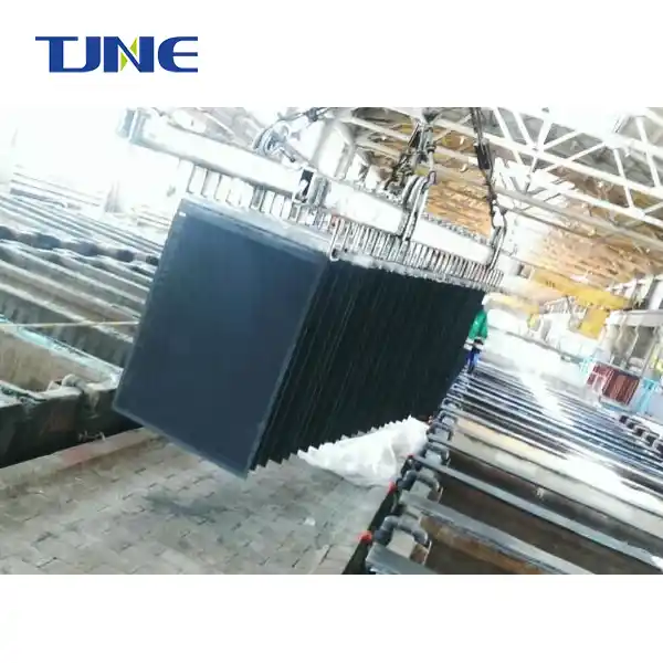
It is a process that involves the deposition of a layer of gold on the surface of PCBs. This plating technique enhances the conductivity, corrosion resistance, and solderability of the PCBs. It is crucial for creating reliable electronic connections and ensuring the overall performance of the PCBs.
Working Principle and Chemical Performance
The gold plating process is based on electrochemical principles. It involves the use of a gold electrolyte solution and the application of an electric current to facilitate the deposition of gold ions onto the PCB's surface. The chemical performance of the process ensures that the gold layer is uniform and adheres firmly to the PCB, providing excellent conductivity and protection against oxidation.
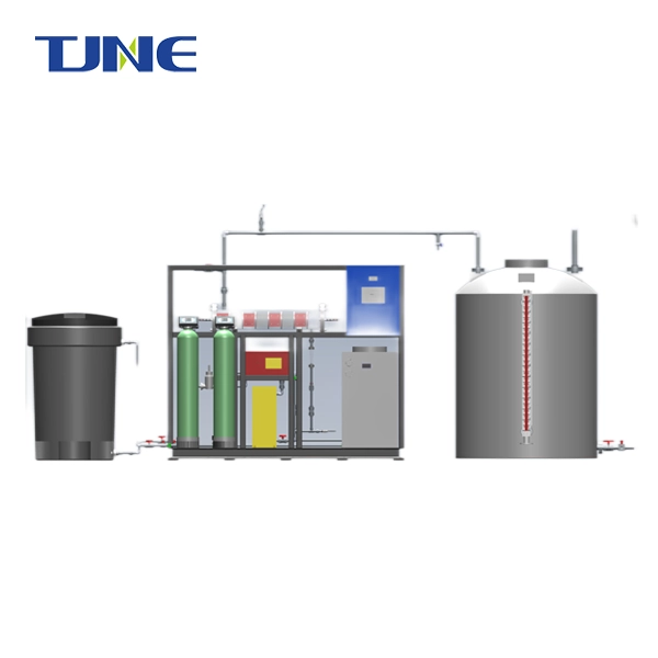
System Composition and Structure
It consists of several components, including a gold plating tank, power supply, rectifier, PCB holding fixtures, and a control panel. The tank houses the gold electrolyte solution, while the power supply and rectifier deliver the necessary voltage and current for the plating process. The PCB holding fixtures securely hold the PCBs during plating, and the control panel allows for precise control and monitoring of various parameters.
Structural Characteristics
-
High-quality gold plating with excellent adhesion
-
Uniform gold layer thickness for consistent performance
-
Improved solderability for easy assembly
-
Enhanced conductivity for reliable electronic connections
-
Corrosion resistance for prolonged PCB lifespan
Performance Parameters
| Parameter | Value |
|---|---|
| Gold layer thickness | 2-5 microns |
| Plating speed | 10-20 μm/h |
| Plating uniformity | ±5% |
| Corrosion resistance | Up to 1000 hours (salt spray test) |
Technical Parameters
| Parameter | Value |
|---|---|
| Power supply voltage | 220V/380V |
| Power supply frequency | 50Hz/60Hz |
| Max. plating area | 500mm x 500mm |
| Temperature range | 10-60°C |
Economic Indicators
| Parameter | Value |
|---|---|
| Plating cost | Low |
| Production efficiency | High |
| Plating quality | High |
Special Features
-
Complete one-stop after-sales service
-
Comprehensive certification and testing reports
-
Fast delivery and secure packaging
-
Support for testing and evaluation
Applications
PCB Gold Plating DSA is ideal for a wide range of applications, including:
-
Consumer electronics
-
Telecommunications
-
Automotive
-
Industrial equipment
-
Medical devices
Gold plating of printed circuit boards (PCBs) is critical for enhancing conductivity and corrosion resistance. However, traditional gold plating methods can have quality issues like non-uniform thickness and poor bonding. The PCB Gold Plating DSA system provides precision control for optimal gold layer properties.
benefits:
1. Digital switching amplifier enables accurate current regulation for consistent gold deposition.
2. Closed loop controls of solution parameters prevent defects like burnt deposits.
3. Advanced anode activation and solution misting give high-speed plating.
4. Robust mechanical hardware design improves reliability.
5. Automatic replenishment system maintains precise bath chemistry.
6. Touchscreen HMI allows easy monitoring and process adjustment.
7. Modular configurations suit different production volumes.
8. Complies with stringent aerospace and military quality standards.
With its precision digital controls and optimized hardware, the PCB Gold Plating DSA system improves bonding strength, uniformity, and repeatability compared to traditional DC plating methods. By preventing over-deposition and other defects, it enhances yields for fine line PCBs in consumer devices, while meeting quality needs for mission-critical aerospace and defense applications.
FAQ
1. Can PCB Gold Plating be used with different PCB sizes?
Yes, the system can accommodate PCBs with a maximum size of 500mm x 500mm.
2. How long does the gold-plated layer last?
The gold-plated layer can withstand up to 1000 hours of salt spray test, ensuring long-lasting performance.
3. Can you provide technical support for the plating process?
Yes, our technical team is available to provide support and guidance for the plating process.
Contact Us
If you are looking for your own PCB Gold Plating system, please feel free to contact us at yangbo@tjanode.com.
TJNE is your reliable partner for PCB Gold Plating DSA solutions!